
For over half a century, silicon (Si) has been the undisputed king of the semiconductor world. It is the material foundation upon which the entire modern digital age was built. However, as we push the boundaries of power efficiency, charging speeds, and renewable energy integration, silicon is beginning to hit its physical limits. We are now entering the era of Wide Bandgap (WBG) semiconductors, led by two revolutionary materials: Silicon Carbide (SiC) and Gallium Nitride (GaN). These materials are not just incremental improvements; they are transformative technologies enabling the electric vehicle (EV) revolution, the rollout of 5G, and the modernization of the electrical grid. But for electronics manufacturers, adopting SiC and GaN is not as simple as swapping one chip for another. These advanced materials introduce unique physical characteristics that demand new manufacturing strategies and precise assembly processes. At BENCOR, we are at the forefront of this shift, adapting our US-based manufacturing lines to handle the distinct requirements of these next-generation components.
Beyond Silicon: Why the World is Switching to WBG
To understand the manufacturing challenge, one must first understand why the industry is making this expensive and complex transition. Silicon has served us well, but it struggles with high voltages and high temperatures, and it loses efficiency as switching speeds increase.
The Power of the "Wide Bandgap"
The term “bandgap” refers to the energy required to free an electron in the semiconductor material. SiC and GaN have a much wider bandgap than silicon. This property allows them to operate at much higher voltages, temperatures, and frequencies. For an engineer, this means smaller capacitors and inductors can be used, shrinking the overall size of power supplies and inverters dramatically while increasing energy efficiency.

Silicon Carbide (SiC): The Heavy Lifter
SiC is the material of choice for high-power, high-voltage applications. It is exceptionally hard and robust. You will find SiC replacing silicon IGBTs in EV traction inverters, EV charging stations, and large-scale solar inverters. It excels at handling the massive power flows required to drive a car or power a neighborhood.

Gallium Nitride (GaN): The Speed Demon
GaN is renowned for its electron mobility, allowing for incredibly fast switching speeds. This makes it ideal for high-efficiency consumer electronics chargers (making your laptop brick tiny), RF power amplifiers for 5G base stations, and data center power supplies.

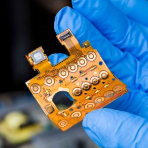
The Manufacturing Implications: It's Not a Drop-In Replacement
While SiC and GaN offer incredible performance benefits, they are not “drop-in” replacements for silicon in the assembly process. They introduce specific challenges that a Contract Electronics Manufacturer (CEM) must be equipped to handle.
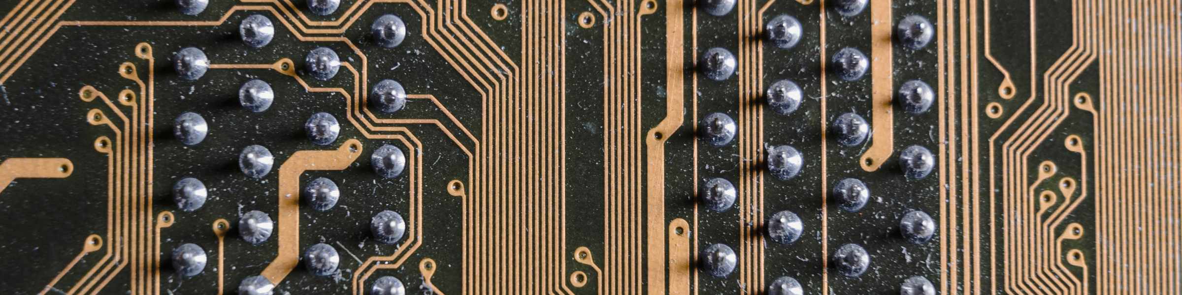
Thermal Management and Solder Joint Reliability
Because these components can operate at much higher temperatures (often exceeding 175°C or even 200°C), standard solder alloys are often insufficient. Traditional SAC305 solder may soften or fatigue under these extreme thermal cycles. Manufacturing with SiC often requires the use of advanced high-reliability solder alloys (like Innolot) or, in extreme cases, the use of silver sintering technology. Sintering is a complex process that creates a stronger thermal and electrical bond than soldering but requires specialized equipment and pressure application that standard SMT lines do not possess.

Fragility and Handling of GaN
While SiC is mechanically tough, GaN dies can be brittle. Furthermore, GaN is often packaged in incredibly small, chip-scale packages (CSP) with very fine pitches to minimize parasitic inductance. This requires extremely precise pick-and-place machines with low placement force control. If the nozzle hits the component too hard during placement, the GaN crystal can crack. BENCOR ensures our SMT equipment is calibrated for this level of delicacy.

Reflow Profiling Sensitivity
The thermal mass of these new packages differs from traditional silicon. Because WBG devices are often smaller but run hotter, the reflow profile must be meticulously tuned. The ramp-up and cool-down rates must be controlled to prevent thermal shock, especially since these components are often mounted on metal-core PCBs (MCPCBs) or heavy copper boards to aid in heat dissipation. A standard profile used for a silicon chip might result in voids or cold solder joints on a SiC device.

Design for Manufacturing (DFM) for WBG
The transition to SiC and GaN also changes the rules for PCB layout. Because these switches operate so fast, they generate steep voltage transients (high dv/dt). This means that stray inductance in the PCB layout can cause massive voltage spikes and electromagnetic interference (EMI).
At BENCOR, our DFM review process looks specifically for these issues. We work with our customers to ensure that the layout minimizes loop inductance and that the thermal path is sufficient to handle the heat density of these powerful chips. We check that the pad designs are optimized not just for electrical connection, but for self-alignment during reflow and maximum thermal transfer.
BENCOR: We are Ready for the High-Voltage Future
The adoption of SiC and GaN is a critical step in maintaining American technological leadership in green energy and advanced mobility. However, the performance of these expensive components is entirely dependent on the quality of their assembly. A poorly soldered SiC MOSFET in an EV inverter is a failure point that can strand a vehicle.
BENCOR has invested in the training and equipment necessary to support this WBG revolution. We understand the specific metallurgical and mechanical requirements of these advanced materials. By partnering with a US-based manufacturer that stays ahead of the technology curve, you ensure that your next-generation power electronics are built to last. We don’t just assemble boards; we help you unlock the full potential of Silicon Carbide and Gallium Nitride, reliably and efficiently.
Conclusion
The shift from silicon to Silicon Carbide and Gallium Nitride is one of the most significant hardware transitions of the 21st century. It promises a greener, faster, and more efficient future. However, realizing this promise requires a manufacturing partner who understands that these new materials demand new processes. From specialized solder alloys to precision placement and thermal profiling, BENCOR has the expertise to handle the complexities of WBG manufacturing. Let us help you power the future with the quality and reliability that only American manufacturing can provide.