In the intricate universe of electronics manufacturing, the solder joint is the fundamental building block of connection. It is both the electrical bridge that allows signals to flow and the mechanical anchor that holds components firmly in place. The long-term reliability of any electronic device, from a simple consumer gadget to a life-critical medical instrument, depends on the integrity of thousands of these microscopic connections. While we often focus on component selection and circuit design, the ultimate success of a solder joint is determined by its foundation: the PCB pad, or land pattern. This seemingly simple area of exposed copper on the Printed Circuit Board is, in fact, a meticulously engineered feature whose design has a profound and direct impact on manufacturing yields, product performance, and long-term durability. At BENCOR, we understand that this microscopic attention to detail is a hallmark of superior manufacturing, and it’s a commitment we bring to every American-made assembly we produce.
What is a PCB Pad (Land Pattern)? The Foundation of Connection
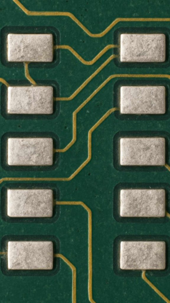
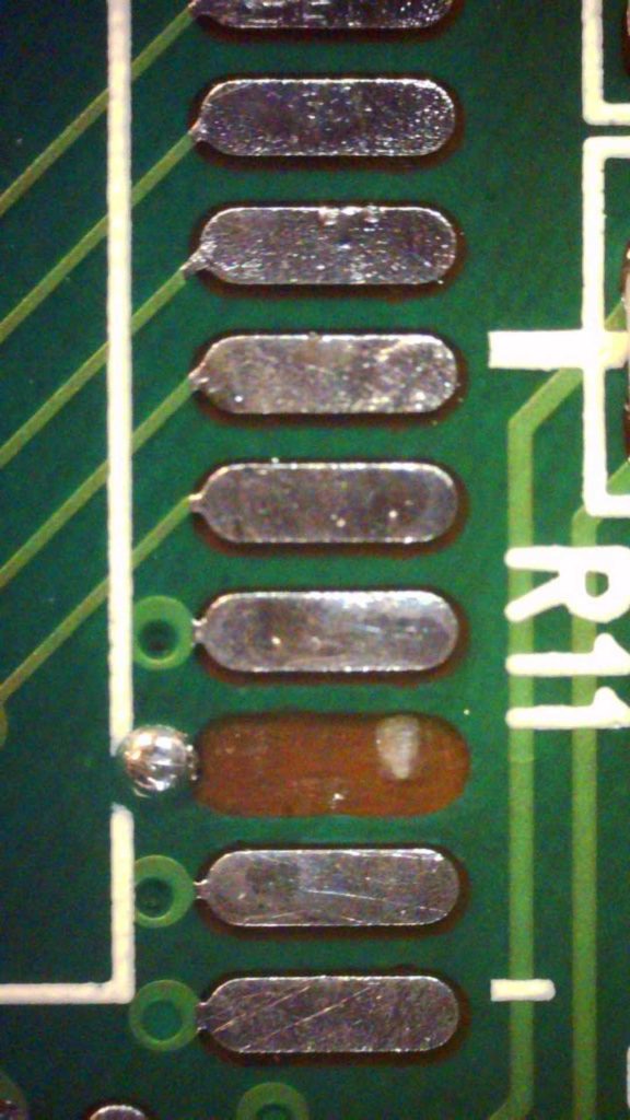
A PCB pad, more formally known as a land pattern, is the exposed surface area of copper on a circuit board where the lead (or termination) of an electronic component is soldered. Each component on a board, whether it’s a tiny two-terminal resistor or a complex Ball Grid Array (BGA) with hundreds of connections, has a corresponding set of pads designed specifically for it.
This pattern serves two critical functions simultaneously. Electrically, it is the designated terminal for the solder to connect the component to the desired trace or plane within the circuit. Mechanically, it provides the surface area for the solder to adhere to, physically securing the component to the board and enabling it to withstand shock, vibration, and thermal stresses throughout its operational life. The design of these pads is governed by industry standards, most notably IPC-7351 (Generic Requirements for Surface Mount Design and Land Pattern Standard), which provides a systematic methodology for creating reliable land patterns.
The Physics of a Perfect Solder Joint: Why Pad Design is Paralyzingly Important
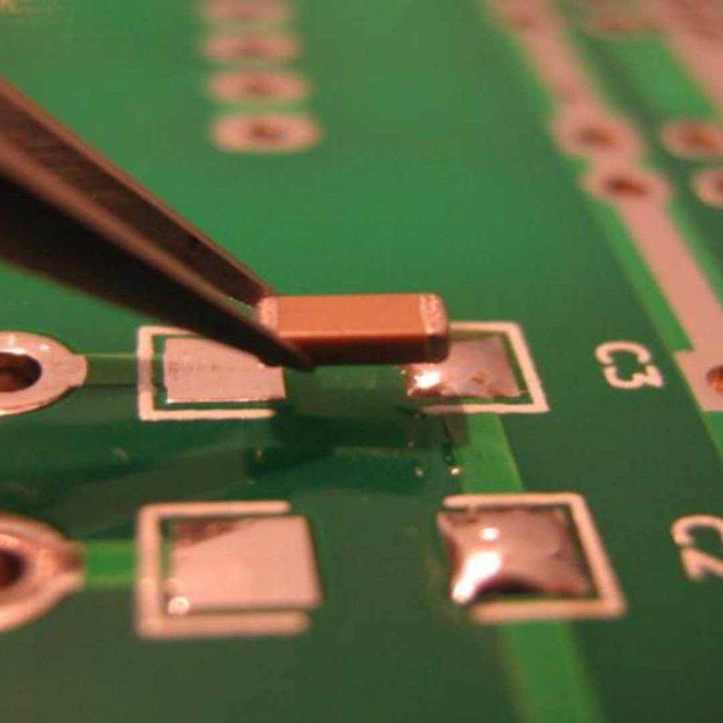
To appreciate why pad design is so critical, one must understand the physics of the solder reflow process. During SMT assembly, solder paste (a mixture of tiny solder spheres and flux) is printed onto the pads. When the board passes through a reflow oven, this paste melts into a liquid state. The powerful force of surface tension in the molten solder then goes to work, pulling the solder into a predictable, minimum-energy shape around the component lead and the PCB pad. This final, solidified shape is known as the solder fillet.
Achieving the Ideal Solder Fillet
A perfect solder fillet has a smooth, concave shape that indicates good “wetting” – the molten solder has bonded well to both the component lead and the PCB pad surfaces. This ideal shape provides the strongest possible mechanical bond and the most reliable electrical connection. The size and geometry of the PCB pad directly influence the volume of solder paste deposited and, crucially, guide the surface tension forces that form this fillet. In essence, the pad design is the architectural blueprint for the final solder joint.
The Dangers of Poor Pad Design
When the pad design is not optimized, those same powerful surface tension forces can work against you, leading to a host of common and costly manufacturing defects:
- Tombstoning: This is a classic defect affecting small, two-terminal passive components like resistors and capacitors. If the pads on either side of the component are different sizes, one pad will heat up faster or have a stronger surface tension pull, causing the molten solder to lift one side of the component into the air, making it resemble a “tombstone.”
- Solder Bridging: If pads for adjacent component pins are designed too wide or too close together, the molten solder can easily flow between them, creating an unintended electrical short circuit. This is especially critical for fine-pitch components.
- Insufficient Solder (Opens): Conversely, if pads are designed too small, they may not hold a sufficient volume of solder paste to form a robust and complete connection, leading to weak joints or open circuits that may not be detected until final testing or, worse, fail in the field.
- Solder Balling: An improper relationship between the pad size and the solder mask opening can cause small spheres of solder to detach from the main joint during reflow, potentially causing shorts elsewhere on the board.
- Reduced Mechanical Strength: Incorrect pad geometry can result in a poorly formed fillet, leading to a weak joint that is highly susceptible to cracking and failure when exposed to mechanical vibration, shock, or thermal cycling.
Key Elements of Effective Pad Design
Creating a reliable land pattern involves more than just making a copper rectangle. Several key elements must be carefully considered by the PCB designer.
Toe, Heel, and Side Fillets
For standard chip components and leaded components (like gull-wing leads on a QFP), the pad must extend beyond the component termination in three directions to promote the formation of proper fillets. The toe is the portion of the pad extending outward from the component. The heel is the portion extending inward, underneath the component body. The side fillets form along the sides of the termination. Having the correct pad extension in each of these areas is crucial for creating a strong joint and, just as importantly, for allowing visual inspection (both human and automated) of the solder joint’s quality.
Solder Mask Definition: SMD vs. NSMD
The interaction between the copper pad and the solder mask opening around it is a critical design choice.
- SMD (Solder Mask Defined): In this configuration, the solder mask opening is intentionally made smaller than the copper pad underneath. The solder mask, therefore, defines the precise area where solder can bond. This is often used for high-density, fine-pitch BGAs because the web of solder mask between the pads can help prevent solder bridging.
- NSMD (Non-Solder Mask Defined): This is the more common and generally preferred method for most components. The solder mask opening is larger than the copper pad. This allows the solder to wet not only to the top surface of the pad but also to its vertical sides, providing a stronger, more reliable mechanical anchor.
Thermal Relief for Connections to Large Copper Planes
Connecting a component pad directly to a large copper ground or power plane can create a significant manufacturing problem. The plane acts as a massive heat sink, drawing thermal energy away from the pad so quickly that the solder paste may not reach its full liquidus temperature during reflow. This results in a cold, weak, or incomplete solder joint. To prevent this, thermal relief pads are used. These connect the pad to the plane using several small copper spokes, which create a thermal barrier to allow the pad to heat up properly while still providing a robust electrical connection.
Adhering to Datasheets and Industry Standards
Component manufacturers provide immense value in their datasheets, including a recommended land pattern for each specific part. This should always be the designer’s starting point, as it is based on the component’s exact dimensions and thermal properties. Additionally, the IPC-7351 standard provides a comprehensive, systematic framework for calculating optimal pad dimensions based on component tolerances and desired solder joint goals, helping to standardize best practices across the industry.
The Role of Your CEM: Manufacturing-Aware Pad Design
While the initial responsibility for pad design lies with the design engineer, an experienced Contract Electronics Manufacturer (CEM) plays a crucial partnership role in ensuring those designs translate into reliable products.
Invaluable Design for Manufacturability (DFM) Feedback
A design that looks perfect in a CAD tool may present challenges on a specific manufacturing line. Even standard library footprints may need slight modifications to be optimized for a CEM’s particular equipment, such as their solder paste stencil technology or reflow oven capabilities. This is where BENCOR’s DFM review process becomes invaluable. Our experienced engineers review customer land patterns to identify potential issues—like insufficient thermal relief, pads that are too close for our assembly tolerances, or other manufacturability risks—before the first board is ever fabricated. This proactive feedback loop saves our customers time, money, and prevents costly board respins.
Deep Process and Quality Control Expertise
A world-class CEM understands the intricate dance between pad design, stencil aperture design, solder paste chemistry, and the thermal reflow profile. BENCOR’s deep process knowledge, honed over decades of manufacturing, ensures that we can optimize our processes to achieve the best possible solder joint quality for a given pad design, delivering consistency and reliability from the first board to the ten-thousandth.
The American Commitment to Microscopic Detail
This intense focus on details that are often invisible to the naked eye is a defining characteristic of high-quality American manufacturing. It is a commitment rooted in the understanding that long-term product reliability is built upon a foundation of countless, perfectly executed microscopic details. This pride in craftsmanship, ensuring that even the smallest pad is designed and processed for optimal performance, is a core part of BENCOR’s philosophy. We don’t just build assemblies; we build confidence.

Conclusion: The PCB pad is far more than a simple copper shape; it is a carefully engineered foundation that dictates the strength, conductivity, and ultimate reliability of every solder joint on a board. Proper pad design, guided by industry standards and an understanding of the physics of soldering, is a first-line defense against a wide range of common manufacturing defects. To truly ensure success, this design knowledge must be paired with the practical expertise of an experienced manufacturing partner. BENCOR stands as that expert American partner, whose rigorous DFM review and deep process knowledge ensure that your thoughtful designs are transformed into flawlessly assembled, highly reliable electronic products, built to last.


