
For decades, the relentless rhythm of the electronics industry has been dictated by Moore’s Law, the famous observation that the number of transistors on a microchip doubles approximately every two years. This principle drove the creation of ever-more-powerful, single-piece, monolithic System-on-a-Chip (SoC) designs. But as we push against the very limits of physics and economics at the most advanced manufacturing nodes, this traditional path is becoming increasingly challenging. The era of simple scaling is evolving.
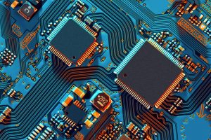
Welcome to the Chiplet Revolution, a new paradigm poised to define the next generation of high-performance computing. This modular approach, which involves combining smaller, specialized silicon dies (chiplets) into a single package, is enabling unprecedented levels of performance and flexibility. However, this entire revolution hinges on an often-unsung hero: the advanced Printed Circuit Board (PCB) substrate or interposer that connects them all. As a dedicated American manufacturer focused on the future, BENCOR understands that our role in expertly assembling these complex systems is more critical than ever in supporting our nation’s technological leadership.
The End of an Era: Why Monolithic Chips Are Facing a Wall
For years, the goal was to integrate as much functionality as possible onto a single, large piece of silicon. This monolithic approach, however, faces fundamental challenges in the mid-2020s.
The Yield Problem
As a monolithic chip grows in size to accommodate more cores and features, the probability of a single, microscopic defect occurring somewhere on the die increases dramatically. Even one such flaw can render the entire multi-million-dollar chip useless. This crushes manufacturing yields (the percentage of good chips per wafer) and drives the cost of functional, large-die chips astronomically high.
The Escalating Cost of Advanced Nodes
Designing and fabricating a chip on the latest process nodes (e.g., 3nm, 2nm) is an incredibly expensive endeavor, costing hundreds of millions of dollars. From a business standpoint, it makes little economic sense to build relatively simple functions, like I/O controllers or memory interfaces that don’t benefit from the latest scaling, on the same expensive, cutting-edge silicon as a high-performance CPU or AI accelerator core.
Inflexible Design
A monolithic design locks all the chip’s functions into a single process node. This “one-size-fits-all” approach lacks the flexibility to use the most appropriate and cost-effective manufacturing process for each specific function.

Enter the Chiplet: A Modular Approach to High-Performance Silicon
The chiplet model elegantly solves these challenges by breaking up the monolithic chip into a set of smaller, specialized, and interoperable blocks. Think of it as building a high-performance engine using specialized, best-in-class components (pistons, fuel injectors, turbochargers) rather than trying to carve the entire engine from a single, massive block of metal.

Improved Yield and Optimized Costs
Because each individual chiplet is much smaller than a large monolithic die, the manufacturing yield for each one is significantly higher. If a defect occurs on one chiplet, only that small die is discarded, not the entire system. This model also allows companies to mix and match chiplets made on different, more appropriate process nodes. The high-performance CPU cores can be fabricated on the expensive, leading-edge 2nm node, while the I/O controllers can be made on a more mature and cost-effective 7nm or 12nm node, optimizing the cost of the entire package.
Unprecedented Flexibility and Faster Time-to-Market
Companies can now develop a library of validated chiplets (CPU, GPU, AI, I/O, memory, etc.) that can be combined in various configurations to create a wide portfolio of products. A new server CPU or a consumer-grade processor can be developed by rearranging these proven “LEGO bricks,” dramatically accelerating the design cycle and time-to-market compared to designing a new monolithic SoC from scratch for each product.
Best-of-Breed" Technology Integration
This modular approach allows for the integration of the best possible technology for each function. A company could, for example, combine its own high-performance CPU chiplets with GPU chiplets from another leading vendor and I/O chiplets from a third specialist, all within a single, powerful package.
The Unsung Hero: Advanced PCB Substrates and Interposers
This entire modular revolution is only possible because of the incredibly sophisticated platform that connects these chiplets together. For chiplets to communicate with each other at ultra-high speeds as if they were on the same piece of silicon, they require an interconnect fabric with extremely high density. This is the critical role played by advanced PCB substrates and, in some cases, even more advanced interposers. They are the “mini-motherboards” that form the heart of the system.
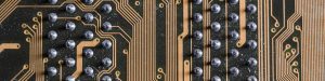
Advanced PCB Substrates
When we talk about substrates in this context, we are not referring to a standard green motherboard. These are highly advanced organic PCBs, often featuring multiple “build-up” layers of dielectric material and copper. They utilize fabrication techniques far beyond standard PCBs, achieving incredibly fine lines and spaces (often just a few microns wide) and employing a dense array of microvias to route thousands of connections between the chiplets and to the larger package that will be soldered onto the final product’s main PCB.
Silicon and Glass Interposers
For the most demanding applications requiring the absolute highest interconnect density, an interposer is used. An interposer is a very thin, intermediate layer—often made of silicon (like a chip) or glass—that sits between the chiplets and the organic substrate. It acts as a high-density bridge, offering ultra-fine wiring that is even denser than what advanced organic substrates can achieve. This enables what is known as 2.5D packaging, where multiple chiplets are placed side-by-side on top of the interposer.
Key Technological Challenges
Creating these interconnect platforms is a technological marvel facing immense challenges:
- Ultra-High Density: Managing and routing thousands of high-speed connections in a space often smaller than a postage stamp requires extreme precision.
- Signal Integrity: Ensuring that data signals remain clean, without distortion or interference, as they travel at terabits per second between chiplets is a monumental engineering task.
- Power Integrity: Delivering stable, noise-free power to a dozen or more different chiplets, each with unique power requirements, is incredibly complex.
- Thermal Management: Effectively removing the concentrated heat from this dense collection of powerful silicon is critical to prevent overheating and ensure reliable operation.

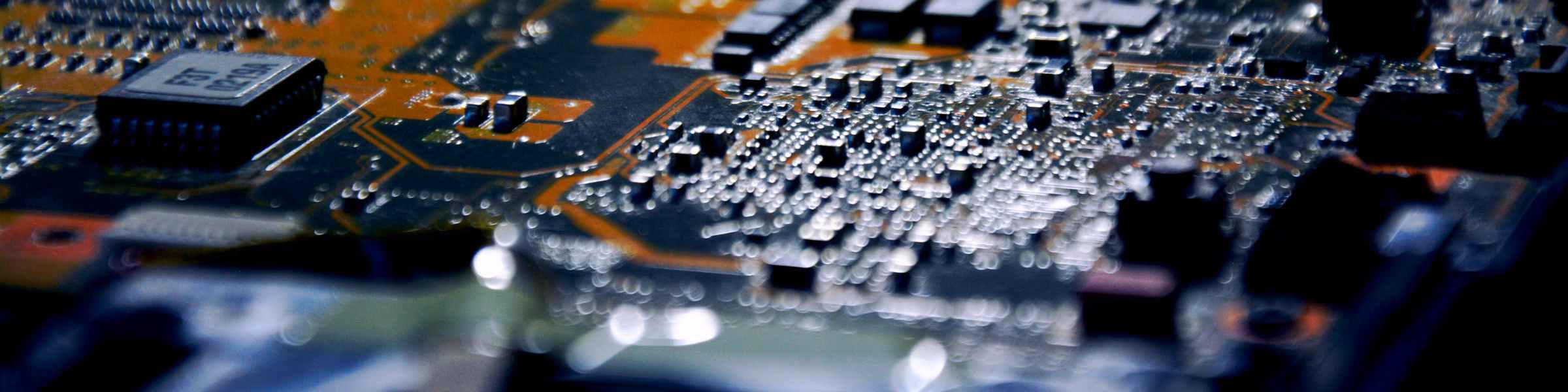
BENCOR's Role in the Chiplet Ecosystem: Assembling the Future
While BENCOR does not fabricate semiconductor chiplets or silicon interposers, our role in this ecosystem is absolutely critical: we are the experts who assemble these highly complex and valuable packages onto the final product’s main PCB. As this chiplet-based technology, often delivered in the form of a System-in-Package (SiP) module, becomes more prevalent, the demands on the electronics assembly process increase exponentially.
Conclusion: The shift from monolithic chips to the flexible, powerful, and cost-effective chiplet model marks a true inflection point for the semiconductor industry. This revolution, born from the need to push beyond the traditional limits of Moore’s Law, is entirely enabled by the parallel and equally impressive advancements in high-density PCB substrates and interposers. As these powerful, modular packages become the new standard in high-performance computing, the expertise required to reliably assemble them onto final products becomes more critical than ever. BENCOR is proud to stand ready, with the advanced capabilities, quality systems, and deep experience needed to support American innovation in this new and exciting era of electronics.