
The relentless drive towards smaller, faster, and more powerful electronic devices is fueling a constant need for miniaturization in the world of Printed Circuit Boards (PCBs). Consumers and industries alike demand products that pack more functionality into ever-shrinking form factors. This trend is pushing the boundaries of traditional PCB manufacturing techniques, making technologies like microvias and High-Density Interconnect (HDI) essential for modern electronic design.
What are Microvias?
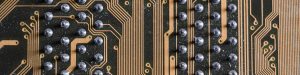
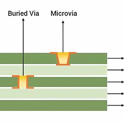
Microvias are small, laser-drilled or chemically etched vias (holes that connect different layers of a PCB) with a diameter typically less than 150 micrometers (µm) – often much smaller. Compare this to traditional mechanically drilled vias, which can be several times larger. This smaller size allows for significantly higher connection density, enabling more components and traces to be packed onto a smaller PCB area. There are several types of microvias:
Blind Vias: Connect an outer layer of the PCB to one or more inner layers, but do not go through the entire board.
Buried Vias: Connect two or more inner layers, but do not reach either of the outer layers. They are completely hidden within the PCB structure.
Stacked Vias: Consist of multiple microvias stacked directly on top of each other, creating a continuous connection through multiple layers. This further increases connection density.
Staggered Vias: Similar to stacked vias, but the individual microvias are slightly offset from each other. This can improve reliability and reduce stress on the PCB.

What is High-Density Interconnect (HDI)?
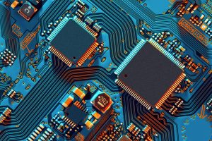
HDI is a PCB manufacturing methodology that utilizes microvias, along with other advanced techniques, to achieve extremely high wiring density and component density. HDI PCBs typically have:
- Finer Traces and Spaces: Smaller trace widths and smaller spaces between traces compared to conventional PCBs.
- Higher Layer Counts: More layers to accommodate the increased routing complexity.
- Sequential Lamination: HDI boards are often built using sequential lamination, where layers are added and processed one or two at a time, allowing for the creation of blind and buried vias.
Advantages of Microvias and HDI
The use of microvias and HDI technology offers numerous benefits for electronic design:
Miniaturization: The most obvious advantage is the ability to significantly reduce the size and weight of PCBs. This is crucial for portable devices, wearables, and other applications where space is at a premium.
Increased Component Density: Microvias and finer traces allow for the placement of more components on a given board area. This enables greater functionality and more complex circuits.
Improved Signal Integrity: Shorter signal paths and reduced via stub lengths (the portion of a via that extends beyond the signal layer) improve signal integrity, particularly at high frequencies. This reduces signal loss, reflections, and crosstalk.
Enhanced Thermal Management: Microvias can be used to create thermal vias, which help to dissipate heat from components, improving the overall thermal performance of the PCB.
Reduced Layer Count: In some cases, the use of microvias and HDI can actually reduce the overall layer count of a PCB, despite the increased complexity. This can lead to cost savings.
Faster Time-to-Market: The ability to create smaller, more powerful devices can accelerate product development cycles.

Applications of Microvias and HDI
Microvia and HDI technology are used in a wide range of applications, including:
- Mobile Devices: Smartphones, tablets, and smartwatches rely heavily on HDI to achieve their compact form factors.
- Wearable Technology: Smartwatches, fitness trackers, and medical devices benefit from the miniaturization and high performance of HDI.
- Aerospace and Defense: HDI is used in avionics, satellite systems, and other demanding applications where reliability and performance are critical.
- Medical Devices: Implantable medical devices, diagnostic equipment, and other medical electronics utilize HDI to achieve small size, high reliability, and biocompatibility.
- High-Performance Computing: Servers, routers, and other high-performance computing systems use HDI to achieve high data transfer rates and processing speeds.
- Automotive Electronics: Advanced driver-assistance systems (ADAS), infotainment systems, and engine control units (ECUs) are increasingly relying on HDI.


BENCOR’s Expertise in Microvia and HDI Technology
BENCOR is a leader in providing advanced PCB design, fabrication, and assembly services, including expertise in microvia and HDI technology. Bencor can assist their clients with:
- Design for Manufacturability (DFM): BENCOR’s engineers work closely with customers to ensure that their HDI designs are optimized for manufacturability, minimizing costs and maximizing yields.
- Material Selection: BENCOR can recommend the appropriate PCB materials for HDI applications, including high-performance laminates and specialized dielectrics.
- Process Control: BENCOR maintains tight control over its manufacturing processes to ensure the precise formation of microvias and the accurate registration of layers.
- Advanced Inspection and Testing: BENCOR utilizes advanced inspection and testing equipment to verify the quality and reliability of HDI PCBs, including automated optical inspection (AOI) and X-ray inspection.
- Turnkey Solutions: BENCOR offers a full range of services, from design and prototyping to full-scale production and assembly, providing a seamless solution for HDI projects.

The Future of Microvias and HDI
As the demand for miniaturization and high performance continues to grow, microvia and HDI technology will become even more prevalent in electronic design. We can expect to see further advancements in materials, manufacturing processes, and design tools, leading to even smaller, more powerful, and more reliable PCBs.
BENCOR is committed to staying at the forefront of these advancements and to providing its customers with the cutting-edge solutions they need to succeed in the ever-evolving world of electronics. If you have a project that requires the benefits of microvia and HDI technology, contact BENCOR today to discuss your requirements and learn how they can help you bring your vision to life. Their team will be happy to help you.