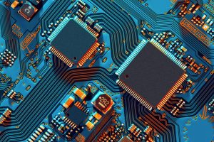

The relentless demand for faster data transmission and processing speeds is driving a fundamental shift in electronic design. From 5G infrastructure and high-performance computing to advanced driver-assistance systems (ADAS) in vehicles, the need for high-speed signal integrity is more critical than ever. This places significant demands on Printed Circuit Board (PCB) design, requiring specialized knowledge, techniques, and tools to overcome the challenges of high-frequency signals.
The Challenges of High-Speed PCB Design
As signal speeds increase, the behavior of electrical signals on a PCB becomes increasingly complex. Effects that are negligible at lower frequencies become major design considerations. Here are some of the key challenges:
Controlled Impedance: At high frequencies, the traces on a PCB act as transmission lines. To prevent signal reflections and ensure efficient power transfer, the impedance of these traces must be carefully controlled. Impedance is determined by the physical characteristics of the trace (width, thickness) and the properties of the surrounding dielectric material. Mismatched impedance can lead to signal loss, distortion, and even device failure.
Crosstalk: Crosstalk is the unwanted coupling of signals between adjacent traces on a PCB. As signal speeds increase, the electromagnetic fields surrounding the traces become stronger, increasing the likelihood of crosstalk. This can lead to data corruption and system instability.
Signal Attenuation (Losses): Signals lose energy as they travel along a PCB trace. This attenuation is due to a combination of factors, including dielectric loss (energy absorbed by the PCB material) and conductor loss (resistance of the trace). At high frequencies, these losses become more significant, limiting the maximum length of traces and requiring careful material selection.
Electromagnetic Interference (EMI): High-speed signals can generate electromagnetic interference, which can disrupt the operation of other electronic devices. Proper PCB design is crucial to minimize EMI and ensure compliance with regulatory standards.
Return Path Discontinuities: The return path for a signal is just as important as the signal trace itself. Discontinuities in the return path (e.g., gaps in the ground plane) can cause impedance mismatches and signal reflections, degrading signal integrity.
Power Delivery Network The increasing density of integrated circuits has increased the power demands and switching speeds of modern digital circuits.
Timing Issues: Skew, the difference in arrival times of a signal on two or more different nets, can become a factor in high speed design, especially when dealing with synchronous interfaces

Techniques for Ensuring Signal Integrity in High-Speed PCB Design
Successfully navigating the challenges of high-speed PCB design requires a combination of careful planning, meticulous layout, and the use of appropriate materials and manufacturing processes. Here are some key techniques:
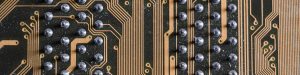
Careful Stackup Design: The PCB stackup (the arrangement of copper layers and dielectric materials) is crucial for controlled impedance and minimizing crosstalk. The thickness and dielectric constant of the materials must be carefully chosen to achieve the desired impedance values.
Trace Width and Spacing: The width of signal traces and the spacing between them are critical parameters that affect impedance and crosstalk. Design rules must be established and strictly followed to ensure signal integrity.
Ground Planes: Solid ground planes are essential for providing a low-impedance return path for signals and for shielding against EMI. Avoid gaps or slots in the ground plane, especially near high-speed traces.
Via Design: Vias (plated holes that connect different layers of the PCB) can introduce impedance discontinuities. Proper via design, including the use of appropriate pad sizes and anti-pads, is important to minimize these effects.
Differential Pair Routing: Many high-speed interfaces use differential signaling, where a signal is transmitted on two traces with opposite polarity. These differential pairs must be routed with tight coupling and controlled impedance to minimize noise and ensure reliable data transmission.
Length Matching: For differential pairs and other critical signals, it’s often necessary to match the lengths of the traces to ensure that signals arrive at their destination at the same time.
Component Placement: The placement of components on the PCB can also affect signal integrity. High-speed components should be placed as close as possible to their associated circuitry to minimize trace lengths.
Simulation and Analysis: Sophisticated software tools are available to simulate and analyze the performance of high-speed PCB designs. These tools can help identify potential problems early in the design process, before the PCB is manufactured.
Power Delivery Network (PDN) design: To ensure the system is able to get the power it needs at the right time, a good PCB designer understands that the PCB layers, traces, and planes all affect PDN performance.

BENCOR’s Expertise in High-Speed PCB Design
BENCOR has extensive experience in designing and manufacturing high-speed PCBs for a wide range of applications. Their team of engineers understands the intricacies of signal integrity and employs best practices to ensure optimal performance. BENCOR’s capabilities include:
- Advanced Design Tools: BENCOR utilizes industry-leading software for schematic capture, PCB layout, and signal integrity simulation.
- Expertise in Controlled Impedance: BENCOR can design PCBs with precise impedance control, meeting the requirements of various high-speed interfaces.
- Experience with Differential Pair Routing: BENCOR has a proven track record of successfully routing differential pairs for high-speed applications.
- Material Selection: BENCOR can recommend and source the appropriate PCB materials for high-speed designs, including low-loss dielectrics.
- Manufacturing Partnerships: BENCOR works with trusted manufacturing partners that have the capabilities to produce high-quality, high-speed PCBs.
- Test fixture design Bencor can offer Test fixture designs, witch are essential for verifying the functionality and performance of PCBs.


The Future of High-Speed PCB Design
As data rates continue to climb, the challenges of high-speed PCB design will only become more demanding. Emerging technologies like PCIe 5.0, DDR5 memory, and 112G SerDes are pushing the boundaries of signal integrity. PCB designers will need to stay abreast of the latest advancements in materials, manufacturing processes, and simulation tools to meet these challenges.
BENCOR is committed to remaining at the forefront of high-speed PCB design and to providing its customers with the expertise and support they need to succeed in this rapidly evolving field. If you have a project that requires high-speed PCB design, contact BENCOR today to discuss your requirements and learn how they can help you achieve your goals. Our team is always ready to respond any question, ensuring the best solutions.