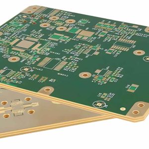
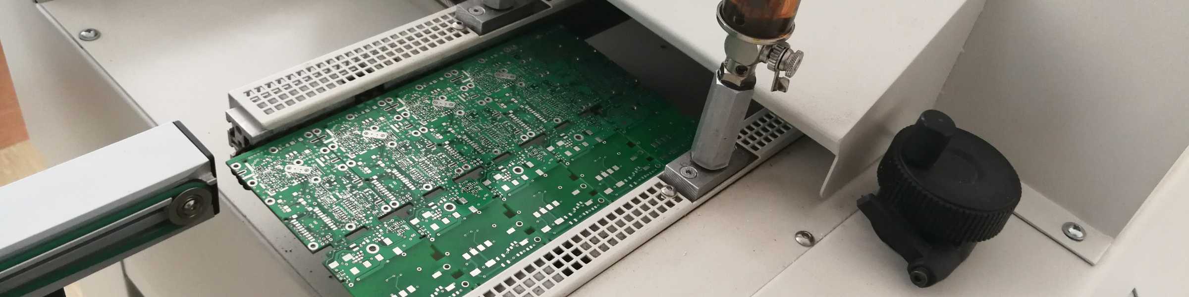

In the world of modern electronics manufacturing, precision is everything. As Printed Circuit Board Assemblies (PCBs) become increasingly dense, complex, and populated with microscopic components, the margin for error shrinks to virtually zero. A single misplaced component, a microscopic solder bridge, or a flawed connection hidden from view can lead to product failure. In this high-stakes environment, relying solely on manual human inspection is no longer feasible; it’s simply too slow, too prone to fatigue, and incapable of detecting the most critical defects. This is where automated inspection technologies become indispensable.
Two of the most powerful tools in a manufacturer’s quality assurance arsenal are Automated Optical Inspection (AOI) and Automated X-Ray Inspection (AXI). While both serve to ensure the integrity of a PCB assembly, they operate on different principles and “see” in fundamentally different ways. Understanding their unique strengths, limitations, and how they work together is key to appreciating what goes into producing a truly reliable electronic product. At BENCOR, our commitment to delivering uncompromising American-made quality means leveraging the right inspection technologies to guarantee that every board we assemble meets the highest standards of excellence.
Automated Optical Inspection (AOI): The Eagle Eye for Surface Defects
Think of Automated Optical Inspection (AOI) as a team of tireless, superhuman inspectors who can scan every square millimeter of a PCB’s surface in seconds. It is a cornerstone of modern SMT (Surface-Mount Technology) production lines, providing a fast and effective first line of defense against common manufacturing defects.
How AOI Works?
An AOI machine uses one or more high-resolution cameras to capture detailed images of a PCB assembly as it passes through the production line. This process is enhanced by sophisticated lighting systems, often using various colors (RGB) and angles to illuminate the board and highlight different features.
The machine’s software then compares these captured images against a pre-defined standard – either a “golden board” (a verified, perfect reference board) or, more commonly, the original CAD and Gerber design data. The software meticulously checks for any discrepancies, flagging potential defects for review by a human operator.
: A Deep Dive into PCB Quality Assurance 1")
Strengths and Capabilities of AOI
OI excels at high-speed, surface-level inspection. Its capabilities are extensive and crucial for process control:
- Component Verification: It can instantly check for the presence or absence of components, verify that the correct component is in the right location, and check for incorrect polarity (e.g., a diode or electrolytic capacitor placed backward) or skew (a component that is misaligned on its pads).
- Solder Joint Inspection (Visible): AOI is excellent at detecting visible solder defects, such as solder bridging (unwanted connections between adjacent pads), insufficient solder, and solder balling. It can also spot common placement issues like component “tombstoning” (where a component stands up on one end) or lifted leads on components like QFPs (Quad Flat Packages).
- Solder Paste Inspection (SPI): A specialized form of AOI, Solder Paste Inspection is often used *before* components are placed and the board is heated. SPI machines scan the solder paste deposits on the bare board to ensure the correct volume and shape of paste is present on every pad, preventing many solder-related defects before they even happen.
- Speed and Efficiency: AOI systems are incredibly fast, making it practical to inspect 100% of the boards coming off a production line without creating a bottleneck. This provides immediate feedback to operators, allowing for rapid process adjustments.
: A Deep Dive into PCB Quality Assurance 2")
Limitations of AOI
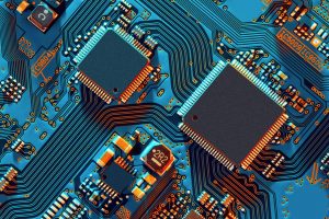
The primary limitation of AOI is fundamental to its nature: it relies on line-of-sight. It can only inspect what its cameras can see from the outside. This means it is completely blind to defects hidden underneath component packages.
AOI cannot see the critical solder joints under Ball Grid Arrays (BGAs), Land Grid Arrays (LGAs), or other bottom-terminated components like many QFNs (Quad Flat No-leads). It also cannot detect internal defects within a solder joint, such as voids (air bubbles). While powerful, AOI only tells part of the quality story.
: A Deep Dive into PCB Quality Assurance 3")
Automated X-Ray Inspection (AXI): Seeing Through to the Solder Joint
When line-of-sight isn’t enough, Automated X-Ray Inspection (AXI) provides the deep, penetrating vision needed to verify the integrity of the most critical and challenging solder connections.
How AXI Works?
An AXI machine generates a low-power beam of X-rays that passes through the entire PCB assembly. A detector on the opposite side captures an image based on the varying densities of the materials the X-rays encounter. Materials with high atomic density, like solder (which contains lead, tin, silver, etc.), absorb more X-rays and appear darker in the image. Materials with low density, like the PCB laminate (fiberglass, epoxy) or component packages (plastic), are largely transparent to the X-rays and appear lighter.
This contrast allows the machine to create a detailed grayscale image of the internal solder structures. More advanced 3D AXI systems can take multiple images from different angles to reconstruct a three-dimensional model, allowing operators to “slice” through a component like a BGA to inspect individual solder balls with incredible detail.
: A Deep Dive into PCB Quality Assurance 4")
Strengths and Capabilities of AXI
AXI’s superpower is its ability to see what is hidden:
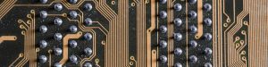
- Inspection of Hidden Solder Joints: This is its most critical application. AXI is the definitive tool for inspecting the solder joints of BGAs, QFNs, and other bottom-terminated components, verifying their shape, size, alignment, and checking for bridging or shorts underneath the package.
- Detection of Internal Solder Defects: AXI can identify a host of internal solder defects that are invisible to AOI, such as voids (air bubbles trapped within the solder, which can compromise reliability), insufficient solder, “head-in-pillow” defects (where the component lead and solder paste fail to coalesce properly), and solder bridging between hidden pads.
- Through-Hole Component Verification: It is also used to verify the quality of through-hole component solder joints by checking the “barrel fill” – ensuring solder has flowed completely through the plated hole to form a strong, reliable connection on both sides of the board.
: A Deep Dive into PCB Quality Assurance 5")
Limitations of AXI
While incredibly powerful, AXI has its own set of trade-offs. The process is significantly slower and more computationally intensive than AOI. As a result, it is often used for process verification, sample-based inspection, or targeted inspection of only the most critical, hidden-joint components on a board, rather than 100% inspection of every component.
The equipment is also more expensive, and analyzing complex X-ray images requires a high level of operator skill and expertise to correctly interpret the results and differentiate between acceptable variations and true defects.
: A Deep Dive into PCB Quality Assurance 6")
AOI and AXI: A Complementary Partnership for Uncompromising Quality
It quickly becomes clear that the debate is not about “AOI vs. AXI,” but rather how to best leverage “AOI and AXI.” They are not competing technologies; they are complementary partners in a comprehensive quality assurance strategy. An effective analogy is airport security: AOI is like the initial boarding pass and ID check – a fast, efficient scan of every passenger for surface-level compliance. AXI is like the detailed baggage X-ray scan – a slower, more intensive look inside to ensure there are no hidden threats. You need both for total security.
In a state-of-the-art manufacturing environment, a typical quality workflow leverages the strengths of each technology at different stages:
- Solder Paste Inspection (SPI): An AOI-based system inspects 100% of boards after solder paste printing to catch defects at the very source.
- Post-Reflow AOI: After components are placed and soldered, another AOI system inspects 100% of the boards to catch placement errors, visible solder defects, and polarity issues.
- Post-Reflow AXI: AXI is then strategically employed to inspect the critical, hidden-joint components like BGAs and QFNs. Depending on the product’s reliability requirements (e.g., for medical, aerospace, or critical industrial controls), this might be done on a sample of boards from each batch or, for the highest-reliability applications, on 100% of the boards.
- Functional Testing (FCT): Finally, after all inspections are complete, the board is powered up and put through a functional test to verify that it actually works as designed.
The BENCOR Commitment: Investing in Quality Assurance You Can Trust
At BENCOR, our philosophy is simple: quality is not a feature to be added; it is the foundation upon which everything is built. We understand that our customers entrust us with their critical designs, and it is our duty to deliver assemblies that are reliable, robust, and built to last. This commitment is why we embrace and utilize advanced inspection technologies like AOI and AXI as integral parts of our manufacturing process.
Leveraging these powerful tools allows us to confidently and consistently assemble highly complex PCBs populated with fine-pitch components, BGAs, and other challenging packages that are impossible to verify by eye alone. This investment in advanced quality assurance is a hallmark of high-quality American manufacturing. It’s about more than just assembling products in the USA; it’s about verifying them to the most stringent standards possible, ensuring the uncompromising reliability that our nation’s critical industries demand. This dedication to process control and verification is a core component of our ISO 9001:2015 certified quality management system, providing our partners with tangible proof of our commitment.
Conclusion: In the intricate landscape of modern PCB assembly, ensuring quality requires vision beyond human sight. Automated Optical Inspection (AOI) provides the speed and efficiency to scrutinize every board’s surface for common defects, while Automated X-Ray Inspection (AXI) offers the penetrating depth needed to guarantee the integrity of critical, hidden solder joints. Together, they form a powerful, complementary strategy for comprehensive quality assurance. Choosing a manufacturing partner who understands, invests in, and expertly utilizes both technologies is crucial for mitigating risks and ensuring the success of any modern electronics project. BENCOR is proud to be that knowledgeable, quality-focused American partner, dedicated to delivering assemblies you can trust, verified inside and out.
: A Deep Dive into PCB Quality Assurance 7")