AI in PCB Layout: How Generative Design is Revolutionizing Board Optimization

AI in PCB Layout: How Generative Design is Revolutionizing Board Optimization

For decades, the process of Printed Circuit Board (PCB) layout has been a testament to human skill and experience. It is a complex digital craft, a multi-dimensional puzzle where engineers meticulously route thousands of connections while balancing a dizzying array of competing physical constraints: signal integrity, power integrity, thermal management, electromagnetic interference (EMI), and Design for Manufacturability (DFM). Using sophisticated CAD tools, a skilled designer iterates—placing, routing, simulating, and rerouting—until they arrive at a solution that works. 

But in an era of skyrocketing data rates, shrinking form factors, and unprecedented complexity, this largely manual, iterative process is beginning to hit its limits. Now, a new frontier is opening, powered by Artificial Intelligence (AI). We are entering the age of Generative Design for PCB layout, a revolutionary approach that transforms the engineer’s role from a digital drafter into the architect of an optimized solution, created in partnership with a powerful AI. As a forward-thinking American manufacturer, BENCOR is keenly watching these developments, understanding that the future of electronics design will demand a new level of manufacturing precision and partnership.

The Limits of Traditional PCB Layout

The expertise of a seasoned PCB layout engineer is invaluable. They rely on years of accumulated knowledge, design rules, and intuition to navigate the complex trade-offs inherent in any modern design. However, even the best designers face inherent limitations imposed by human cognition and the sheer scale of the problem.
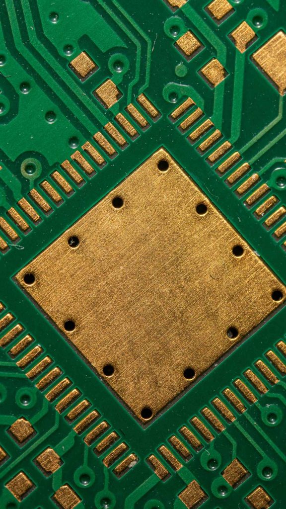
Traditional PCB

The "Good Enough" Problem

Faced with immense complexity and aggressive project deadlines, the goal of a traditional layout process is often to find a solution that successfully meets all the minimum design constraints. An engineer will iterate until they find a layout that passes all simulation checks and DFM rules. While this solution is functional, it is almost certainly not the absolute optimal solution possible. It is simply the first viable path found in a design space containing trillions of possibilities. There may be hundreds of other, better layouts that would yield superior performance or thermal characteristics, but there simply isn’t enough time for a human to explore them.

The Challenge of Competing Constraints

PCB design is a masterclass in managing trade-offs. A component placement that is ideal for minimizing the length of high-speed signal traces might create a thermal hotspot. Routing power planes for optimal power integrity might interfere with sensitive analog signals. A human designer must weigh these competing constraints and make sequential judgment calls based on their experience. It’s a difficult balancing act that rarely results in a truly holistic optimization across all domains simultaneously.

The Astronomical Scale of Possibility

For even a moderately complex PCB, the number of potential routing solutions is astronomical, far exceeding the number of atoms in the known universe. It is physically impossible for a human designer to explore this entire design space. They rely on best practices and established patterns to navigate a tiny fraction of the available options to find a working solution.

Enter Generative Design: A New Partnership Between Human and Machine

Generative Design flips the traditional process on its head. Instead of the engineer manually creating a single solution, they define the problem for the AI, which then explores the vast design space to find the best possible answers. It’s crucial to understand that this is not about AI replacing the engineer. It’s about augmenting their capabilities, freeing them from the tedious task of manual routing to focus on high-level system architecture and goals.

Setting the Goals and Constraints

The engineer acts as the architect, providing the AI with the foundational rules and objectives. This includes the finalized schematic (netlist), the physical board outline, critical component placement zones, and, most importantly, the specific goals and constraints. These can be complex: “achieve 100-ohm differential impedance on these pairs,” “ensure the CPU temperature does not exceed 85°C,” “minimize total trace length for this bus,” and “adhere to these specific DFM rules provided by our manufacturing partner, BENCOR.”

The AI Exploration and Optimization Phase

Once given its instructions, the generative design engine goes to work. Using algorithms inspired by natural evolution, machine learning, and advanced mathematical optimization, it rapidly generates thousands, or even millions, of potential layout and routing solutions. It doesn’t just follow one path; it explores countless possibilities in parallel.

The Evaluation, Learning, and Selection Phase

For each design it generates, the AI automatically runs integrated analysis tools—simulating signal integrity, running thermal analysis, and checking against DFM rules. It instantly discards solutions that fail to meet the constraints. It learns from the successful designs, cross-pollinating positive traits to create new, even better hybrid solutions. Over a period of hours, the AI converges on a set of top-performing, fully-routed designs that represent the optimal trade-offs between all the specified goals. The engineer can then review this curated set of elite options, compare their performance metrics, and use their expert judgment to make the final selection.

AI generative design

How AI-Driven Layout Revolutionizes Board Optimization

The shift from manual layout to AI-powered generative design offers transformative benefits for electronic product development:

True Multi-Objective Optimization

This is perhaps the most significant advantage. Where a human designer often has to optimize for one constraint at a time (e.g., fix signal integrity, then address thermals), an AI can evaluate and optimize for all defined objectives *simultaneously*. It can find the elusive design that represents the best possible balance of electrical performance, thermal management, EMI containment, and manufacturability—a level of holistic optimization previously unattainable.

Unlocking Novel and Non-Intuitive Solutions

AI is not constrained by human habits, biases, or conventional wisdom about “what a good layout looks like.” It may produce routing paths that seem strange or unorthodox to a human eye, but which are provably superior according to the physics-based simulations. It can uncover innovative solutions for component placement or trace routing that a human designer might never have conceived, leading to breakthroughs in performance and board density.

Drastically Reduced Design and Iteration Time

The manual process of routing a complex, high-density board can take a skilled engineer weeks. Generative design can automate this task, reducing the layout phase to a matter of days or even hours. This phenomenal acceleration allows for more design iterations, more time for high-level architectural planning, and a significantly compressed overall product development schedule.

Improved Performance, Reliability, and Yield

Because the final design is more highly optimized from the very beginning, the resulting physical PCB is more likely to perform better. Potential issues with signal integrity, power delivery, EMI, and thermal management are identified and engineered out by the AI before a single board is ever built. This leads to better first-pass success rates, higher manufacturing yields, and a more reliable final product.

Manufacturing Implications: The Role of the CEM in an AI-Driven World

The revolutionary output of an AI design tool still needs to be translated into a physical, reliable product. In this new paradigm, the role of a capable Contract Electronics Manufacturer becomes more critical than ever.

AI driven technology

The Need for a "Digital-Ready" Manufacturing Partner

A CEM must be comfortable and proficient in a fully digital workflow. Partners like BENCOR, who have robust front-end CAM (Computer-Aided Manufacturing) engineering teams, are essential. They have the expertise to take the potentially complex and non-traditional data sets generated by an AI and accurately prepare them for the realities of the factory floor.

The Critical DFM Feedback Loop

The saying “garbage in, garbage out” is especially true for AI. The quality of a generative design is entirely dependent on the quality of the constraints it is given. This is where a close, collaborative partnership between the design team and the manufacturer is vital. An experienced manufacturer like BENCOR can provide a detailed, up-to-date set of real-world DFM rules—our specific capabilities for trace width, spacing, via types, and more. Feeding this precise data into the AI engine ensures that the generated designs are not just theoretically optimal, but are also practical, efficient, and cost-effective to manufacture.

The American Advantage in Building Innovation

The development and adoption of AI-powered design tools represent the very cutting edge of American technological innovation. To fully realize the benefits of these incredibly advanced designs, they must be built by manufacturing partners who operate at an equally high level of precision, quality, and trust. Entrusting an AI-optimized design to a proven, US-based manufacturer like BENCOR ensures that the sophisticated intent of the design is not lost in translation or compromised by substandard processes. It guarantees the highest level of quality control and provides robust protection for the intellectual property contained within America’s most advanced electronic innovations, strengthening our entire domestic technology ecosystem.

Conclusion:

Artificial Intelligence and generative design are poised to fundamentally reshape the landscape of PCB layout, transforming it from a manual art into a sophisticated, collaborative science between the human engineer and an intelligent machine. This powerful partnership promises to deliver truly optimized designs, unlock novel solutions to complex problems, and dramatically accelerate the pace of electronic innovation. However, this design revolution demands a parallel evolution in manufacturing, requiring partners who are digitally fluent, process-driven, and committed to absolute precision. BENCOR is proud to be that forward-looking American manufacturing partner, ready and able to build the complex, AI-optimized designs that will power the future.

You might also enjoy

For decades, the process of Printed Circuit Board (PCB) layout has been a testament to human skill and experience. It is a complex digital craft, a multi-dimensional puzzle where engineers meticulously route thousands of connections while balancing a dizzying array of competing physical constraints: signal integrity, power integrity, thermal management, electromagnetic interference (EMI), and Design for Manufacturability (DFM). Using sophisticated CAD tools, a skilled designer iterates—placing, routing, simulating, and rerouting—until they arrive at a solution that works. 

But in an era of skyrocketing data rates, shrinking form factors, and unprecedented complexity, this largely manual, iterative process is beginning to hit its limits. Now, a new frontier is opening, powered by Artificial Intelligence (AI). We are entering the age of Generative Design for PCB layout, a revolutionary approach that transforms the engineer’s role from a digital drafter into the architect of an optimized solution, created in partnership with a powerful AI. As a forward-thinking American manufacturer, BENCOR is keenly watching these developments, understanding that the future of electronics design will demand a new level of manufacturing precision and partnership.

The Limits of Traditional PCB Layout

The expertise of a seasoned PCB layout engineer is invaluable. They rely on years of accumulated knowledge, design rules, and intuition to navigate the complex trade-offs inherent in any modern design. However, even the best designers face inherent limitations imposed by human cognition and the sheer scale of the problem.

Traditional PCB

The "Good Enough" Problem

Faced with immense complexity and aggressive project deadlines, the goal of a traditional layout process is often to find a solution that successfully meets all the minimum design constraints. An engineer will iterate until they find a layout that passes all simulation checks and DFM rules. While this solution is functional, it is almost certainly not the absolute optimal solution possible. It is simply the first viable path found in a design space containing trillions of possibilities. There may be hundreds of other, better layouts that would yield superior performance or thermal characteristics, but there simply isn’t enough time for a human to explore them.

The Challenge of Competing Constraints

PCB design is a masterclass in managing trade-offs. A component placement that is ideal for minimizing the length of high-speed signal traces might create a thermal hotspot. Routing power planes for optimal power integrity might interfere with sensitive analog signals. A human designer must weigh these competing constraints and make sequential judgment calls based on their experience. It’s a difficult balancing act that rarely results in a truly holistic optimization across all domains simultaneously.

The Astronomical Scale of Possibility

For even a moderately complex PCB, the number of potential routing solutions is astronomical, far exceeding the number of atoms in the known universe. It is physically impossible for a human designer to explore this entire design space. They rely on best practices and established patterns to navigate a tiny fraction of the available options to find a working solution.

Enter Generative Design: A New Partnership Between Human and Machine

Generative Design flips the traditional process on its head. Instead of the engineer manually creating a single solution, they define the problem for the AI, which then explores the vast design space to find the best possible answers. It’s crucial to understand that this is not about AI replacing the engineer. It’s about augmenting their capabilities, freeing them from the tedious task of manual routing to focus on high-level system architecture and goals.

Setting the Goals and Constraints

The engineer acts as the architect, providing the AI with the foundational rules and objectives. This includes the finalized schematic (netlist), the physical board outline, critical component placement zones, and, most importantly, the specific goals and constraints. These can be complex: “achieve 100-ohm differential impedance on these pairs,” “ensure the CPU temperature does not exceed 85°C,” “minimize total trace length for this bus,” and “adhere to these specific DFM rules provided by our manufacturing partner, BENCOR.”

The AI Exploration and Optimization Phase

Once given its instructions, the generative design engine goes to work. Using algorithms inspired by natural evolution, machine learning, and advanced mathematical optimization, it rapidly generates thousands, or even millions, of potential layout and routing solutions. It doesn’t just follow one path; it explores countless possibilities in parallel.

The Evaluation, Learning, and Selection Phase

For each design it generates, the AI automatically runs integrated analysis tools—simulating signal integrity, running thermal analysis, and checking against DFM rules. It instantly discards solutions that fail to meet the constraints. It learns from the successful designs, cross-pollinating positive traits to create new, even better hybrid solutions. Over a period of hours, the AI converges on a set of top-performing, fully-routed designs that represent the optimal trade-offs between all the specified goals. The engineer can then review this curated set of elite options, compare their performance metrics, and use their expert judgment to make the final selection.

AI generative design

How AI-Driven Layout Revolutionizes Board Optimization

The shift from manual layout to AI-powered generative design offers transformative benefits for electronic product development:

True Multi-Objective Optimization

This is perhaps the most significant advantage. Where a human designer often has to optimize for one constraint at a time (e.g., fix signal integrity, then address thermals), an AI can evaluate and optimize for all defined objectives *simultaneously*. It can find the elusive design that represents the best possible balance of electrical performance, thermal management, EMI containment, and manufacturability—a level of holistic optimization previously unattainable.

Unlocking Novel and Non-Intuitive Solutions

AI is not constrained by human habits, biases, or conventional wisdom about “what a good layout looks like.” It may produce routing paths that seem strange or unorthodox to a human eye, but which are provably superior according to the physics-based simulations. It can uncover innovative solutions for component placement or trace routing that a human designer might never have conceived, leading to breakthroughs in performance and board density.

Drastically Reduced Design and Iteration Time

The manual process of routing a complex, high-density board can take a skilled engineer weeks. Generative design can automate this task, reducing the layout phase to a matter of days or even hours. This phenomenal acceleration allows for more design iterations, more time for high-level architectural planning, and a significantly compressed overall product development schedule.

Improved Performance, Reliability, and Yield

Because the final design is more highly optimized from the very beginning, the resulting physical PCB is more likely to perform better. Potential issues with signal integrity, power delivery, EMI, and thermal management are identified and engineered out by the AI before a single board is ever built. This leads to better first-pass success rates, higher manufacturing yields, and a more reliable final product.

Manufacturing Implications: The Role of the CEM in an AI-Driven World

The revolutionary output of an AI design tool still needs to be translated into a physical, reliable product. In this new paradigm, the role of a capable Contract Electronics Manufacturer becomes more critical than ever.

AI driven technology

The Need for a "Digital-Ready" Manufacturing Partner

A CEM must be comfortable and proficient in a fully digital workflow. Partners like BENCOR, who have robust front-end CAM (Computer-Aided Manufacturing) engineering teams, are essential. They have the expertise to take the potentially complex and non-traditional data sets generated by an AI and accurately prepare them for the realities of the factory floor.

The Critical DFM Feedback Loop

The saying “garbage in, garbage out” is especially true for AI. The quality of a generative design is entirely dependent on the quality of the constraints it is given. This is where a close, collaborative partnership between the design team and the manufacturer is vital. An experienced manufacturer like BENCOR can provide a detailed, up-to-date set of real-world DFM rules—our specific capabilities for trace width, spacing, via types, and more. Feeding this precise data into the AI engine ensures that the generated designs are not just theoretically optimal, but are also practical, efficient, and cost-effective to manufacture.

The American Advantage in Building Innovation

The development and adoption of AI-powered design tools represent the very cutting edge of American technological innovation. To fully realize the benefits of these incredibly advanced designs, they must be built by manufacturing partners who operate at an equally high level of precision, quality, and trust. Entrusting an AI-optimized design to a proven, US-based manufacturer like BENCOR ensures that the sophisticated intent of the design is not lost in translation or compromised by substandard processes. It guarantees the highest level of quality control and provides robust protection for the intellectual property contained within America’s most advanced electronic innovations, strengthening our entire domestic technology ecosystem.

Conclusion:

Artificial Intelligence and generative design are poised to fundamentally reshape the landscape of PCB layout, transforming it from a manual art into a sophisticated, collaborative science between the human engineer and an intelligent machine. This powerful partnership promises to deliver truly optimized designs, unlock novel solutions to complex problems, and dramatically accelerate the pace of electronic innovation. However, this design revolution demands a parallel evolution in manufacturing, requiring partners who are digitally fluent, process-driven, and committed to absolute precision. BENCOR is proud to be that forward-looking American manufacturing partner, ready and able to build the complex, AI-optimized designs that will power the future.

You might also enjoy

You might also enjoy