
The Printed Circuit Board (PCB) is the unsung hero of the electronics revolution, the foundational platform upon which virtually all modern technological marvels are built. The process of “printing” these intricate circuit boards – essentially creating the conductive pathways that allow electronic components to communicate and function – has undergone a remarkable evolution since the early days of bulky, simple electronics. Today, the demand for smaller, faster, more powerful, and increasingly complex devices is relentlessly driving innovation in PCB manufacturing technology. Staying abreast of these advancements is crucial for designers, engineers, and any company looking to bring cutting-edge products to market. As a dedicated American manufacturer, BENCOR is committed to leveraging state-of-the-art PCB fabrication techniques, ensuring our partners benefit from the precision, quality, and capabilities that define modern electronics production right here in the USA.
The Foundation: A Brief Look at Traditional PCB Printing
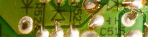
To appreciate the significance of current advancements, it’s helpful to understand the traditional, and still widely used, subtractive method of PCB manufacturing. This process typically begins with a laminate material, most commonly FR-4 (a flame-retardant epoxy resin reinforced with woven fiberglass), clad with a layer of copper. The “printing” involves several key stages:
- Image Transfer (Photolithography): The desired circuit pattern is transferred from a CAD design onto the copper-clad laminate. Traditionally, this involved creating a photomask (a film negative of the circuit). A light-sensitive material called photoresist is applied to the copper. The photomask is placed over the resist-coated board, and the board is exposed to UV light. Where the light passes through the clear areas of the mask, it hardens the photoresist.
- Developing: The unhardened photoresist (the areas shielded by the dark parts of the photomask) is washed away, exposing the underlying copper that needs to be removed.
- Etching: The board is then immersed in an etching solution (typically chemical etchants like ferric chloride or ammonium persulfate) that dissolves the exposed copper, leaving behind the desired conductive copper traces protected by the hardened photoresist.
- Stripping: Finally, the remaining hardened photoresist is stripped away, revealing the copper circuit pattern. Subsequent steps include drilling holes for components, plating through-holes (vias) to connect different layers, applying solder mask, and printing legends.
While this subtractive process is mature, reliable, and cost-effective for many applications, it has inherent limitations, including the generation of chemical waste, potential for undercutting during etching (which can limit trace fineness), and the resolution constraints imposed by using physical film masks.

Key Advancements Revolutionizing PCB Printing Today
The drive for higher performance and miniaturization has spurred significant innovations in how circuit patterns are defined and created on PCBs. These advancements are transforming capabilities and opening new design possibilities.
Direct Imaging (DI) and Laser Direct Imaging (LDI)
Perhaps one of the most impactful advancements has been the widespread adoption of Direct Imaging, particularly Laser Direct Imaging (LDI). Unlike traditional photolithography that uses physical film photomasks, LDI systems transfer the circuit pattern directly from digital CAD data onto the photoresist-coated PCB using a highly focused laser beam or a UV light source modulated by a spatial light modulator (like a DMD chip).
The benefits are substantial:
- Higher Resolution & Finer Features: LDI can achieve significantly finer lines and spaces (down to a few tens of microns) with greater precision than film-based methods, which are susceptible to distortion and alignment errors. This is crucial for High-Density Interconnect (HDI) PCBs.
Improved Registration - Accuracy: Aligning multiple layers in a multi-layer PCB is critical. LDI offers superior layer-to-layer registration, reducing the risk of misalignments.
- Faster Setup for Prototypes & Small Runs: Eliminating the need to create and manage physical films dramatically reduces setup time and cost, especially beneficial for rapid prototyping and low-volume production.
- Reduced Defects: By removing film-related issues like scratches, dust, or handling errors, LDI contributes to higher manufacturing yields.
Additive and Semi-Additive Manufacturing Processes
A paradigm shift from the traditional subtractive method, additive and semi-additive processes build up the conductive traces only where they are needed, rather than etching away unwanted copper.
- Fully Additive: Conductive inks (often containing silver, copper, or carbon nanoparticles) are precisely deposited onto a bare substrate using techniques like specialized inkjet printing or Aerosol Jet Printing. The ink is then cured (sintered) to form the conductive paths.
- Semi-Additive Process (SAP): This typically involves applying a very thin seed layer of copper to the substrate, then imaging a resist pattern, and finally plating up the desired copper thickness only in the exposed areas. The thin seed layer in the unwanted areas is then quickly etched away.
The advantages of these approaches include significantly less material waste (a major environmental benefit), the potential for even finer feature definition, greater design freedom in creating 3D circuit structures, and the ability to use a wider variety of substrate materials, including flexible and stretchable ones. While fully additive processes are still evolving for mainstream high-volume PCB production, SAP is becoming increasingly common for HDI and IC substrate manufacturing.
Advanced Etching and Plating Techniques
Even within subtractive processes, advancements continue. Modern etching chemistries and process controls allow for more anisotropic etching (straighter sidewalls on traces) and significantly reduced undercutting, enabling finer line definition.
Plating technology has also seen significant improvements. Advanced electrolytic and electroless plating processes ensure more uniform copper deposition, crucial for consistent impedance control. Techniques for reliably filling microvias (tiny laser-drilled holes connecting layers in HDI boards) are now standard. Furthermore, a wider array of sophisticated surface finishes (like ENIG – Electroless Nickel Immersion Gold, ENEPIG – Electroless Nickel Electroless Palladium Immersion Gold, and Immersion Tin – ISn) are available, providing superior solderability, shelf life, and reliability for demanding applications like lead-free soldering and fine-pitch component assembly.
Inkjet Printing for Solder Mask and Legend Application
Traditional screen printing for applying solder mask (the protective coating over the copper traces) and legend (component designators and markings) is increasingly being replaced by digital inkjet printing technology. Dedicated inkjet printers can precisely deposit solder mask inks and legend inks directly onto the PCB surface from CAD data.
This offers higher accuracy, the ability to define much finer solder mask dams between closely spaced pads, faster setup times (no screens to create), the capability to print variable data or serialized information, and often a reduction in Volatile Organic Compounds (VOCs) compared to solvent-based screen printing inks.

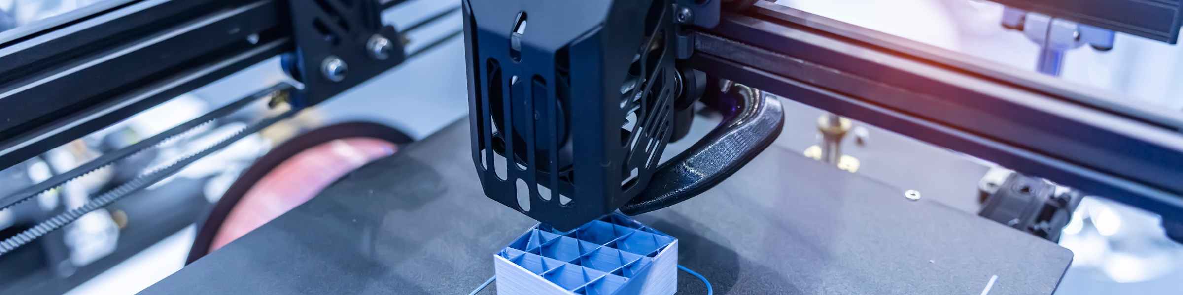
3D-Printed Electronics (A Glimpse into the Future)
While still largely in the research and niche application phase, 3D-Printed Electronics (3DPE) represents a potentially transformative long-term trend. This technology aims to create fully three-dimensional electronic structures, directly printing conductive traces, dielectric materials, and even embedding components within a single, monolithic 3D-printed part. This could revolutionize how products are designed, allowing for integrated mechanical and electrical features in complex, customized shapes.

Impact of These Advancements on PCB Capabilities
These technological leaps in circuit board printing have a profound impact on what is possible in electronic product design:
Increased Density and Miniaturization
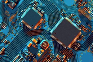
The ability to create finer lines and spaces, smaller vias, and more accurate layer registration directly enables higher component density and overall product miniaturization. This is the driving force behind the sleekness of modern smartphones, the functionality packed into wearables, and the compact nature of advanced medical implants.
Improved Signal Integrity at High Frequencies
As operating frequencies climb into the gigahertz range (e.g., for 5G, 6G, advanced radar, and high-speed digital interfaces), the precision of PCB trace geometries becomes paramount for maintaining signal integrity. Advanced printing techniques provide the control needed to achieve consistent impedance, minimize signal loss, and reduce crosstalk, ensuring reliable performance.
Enhanced Reliability and Manufacturing Yield
Digital processes like LDI and inkjet printing reduce the potential for human error and material variability inherent in older analog methods. Tighter control over etching and plating processes leads to more consistent board characteristics, better via reliability, and ultimately, higher first-pass yields in manufacturing, reducing waste and cost.
Faster Prototyping and Shorter Product Development Cycles
The reduced setup times associated with digital front-end processes (like LDI and inkjet legend/mask) are particularly beneficial for rapid prototyping. Engineers can get physical boards in their hands much faster, allowing for quicker design iterations and a shorter overall product development cycle.
Greater Design Freedom and Innovation
Additive processes and the precision of advanced imaging techniques are opening up new avenues for designers, allowing for more complex trace routing, the integration of features like embedded passives, and the use of novel substrate materials tailored for specific performance requirements.
BENCOR: Harnessing Advanced PCB Printing for American Manufacturing Excellence
At BENCOR, we understand that delivering superior quality Printed Circuit Boards and assemblies begins with leveraging the best available manufacturing technologies. While we may not perform every single one of these advanced printing steps in-house, we partner with leading American PCB fabricators who utilize these state-of-the-art techniques. Our deep understanding of these processes informs our Design for Manufacturability (DFM) reviews, ensuring that the designs we help refine for our customers can be reliably and cost-effectively produced using modern methods.
Our commitment is to ensure that every PCB we procure for your project meets the highest standards of precision and quality demanded by today’s sophisticated electronics. By insisting on advanced fabrication capabilities, we help our customers access the benefits of increased density, improved performance, and enhanced reliability. This dedication to incorporating cutting-edge technology is a cornerstone of American manufacturing excellence. It strengthens our domestic industrial base and ensures that US companies have the onshore capabilities needed to drive innovation and compete globally. When you partner with BENCOR, you’re not just getting an assembly service; you’re gaining a partner committed to the quality and technological superiority that “Made in USA” represents.

Challenges and Considerations with Advanced Printing
While these advancements offer tremendous benefits, they also come with considerations. The capital investment in new equipment like LDI systems or industrial inkjet printers can be substantial. Operating and maintaining these sophisticated machines requires highly skilled personnel. For some of the newer additive technologies, material compatibility, long-term reliability data, and scalability for very high-volume production are still areas of ongoing development and refinement. Furthermore, to fully leverage the capabilities of advanced printing (e.g., ultra-fine lines), the PCB design itself must be meticulously prepared, making robust DFM practices more critical than ever.
Conclusion: The technology behind circuit board printing is far from static; it’s a field of continuous innovation that directly enables the ever-increasing capabilities of modern electronic devices. From the precision of Laser Direct Imaging to the resource efficiency of emerging additive techniques and the finesse of advanced plating, these advancements are pushing the boundaries of what’s possible in PCB design and manufacturing. By understanding and leveraging these technologies, companies can create more compact, powerful, and reliable products. BENCOR is proud to be a knowledgeable American partner, guiding our clients through these complexities and ensuring their projects benefit from the best in modern PCB fabrication and assembly, all while championing the quality and innovation inherent in US manufacturing. Let us help you print the future of your electronic products.