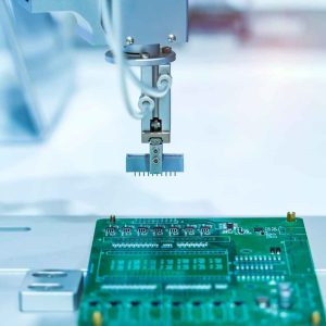

The goal of every Printed Circuit Board (PCB) assembly process is perfection: every component correctly placed, every solder joint flawless, every board functioning exactly as designed. In reality, the path from a bare board to a fully assembled product is a complex interplay of materials, machinery, and physics where, without rigorous process control, defects can occur. Understanding these common assembly defects is the first and most critical step toward preventing them. For design engineers, recognizing how design choices can influence manufacturability is key. For product managers, understanding these issues illuminates the importance of partnering with a high-quality manufacturing expert. This visual guide will explore some of the most common SMT (Surface-Mount Technology) defects, describe what they look like, detail their root causes, and explain how they can be prevented. At BENCOR, we believe that a deep understanding of these challenges is fundamental to the exceptional quality and reliability that defines world-class American manufacturing.
The Importance of Defect Recognition and Prevention
Identifying a defect on the assembly line is crucial, but the true goal is prevention. A seemingly minor cosmetic issue, like a small solder ball, could be an indicator of a deeper process problem. More critically, a defect like an insufficient solder joint might pass an initial functional test only to fail prematurely in the field, leading to costly warranty returns and damage to your brand’s reputation. Many of these potential defects can be significantly minimized or eliminated entirely during the PCB design phase. This highlights the importance of a collaborative partnership between the designer and the manufacturer, where Design for Manufacturability (DFM) feedback is shared and implemented, setting every project up for success before the first component is ever placed.
A Gallery of Common SMT Assembly Defects
Let’s take a closer look at some of the common defects that automated inspection systems and skilled technicians are trained to find, and understand what causes them.
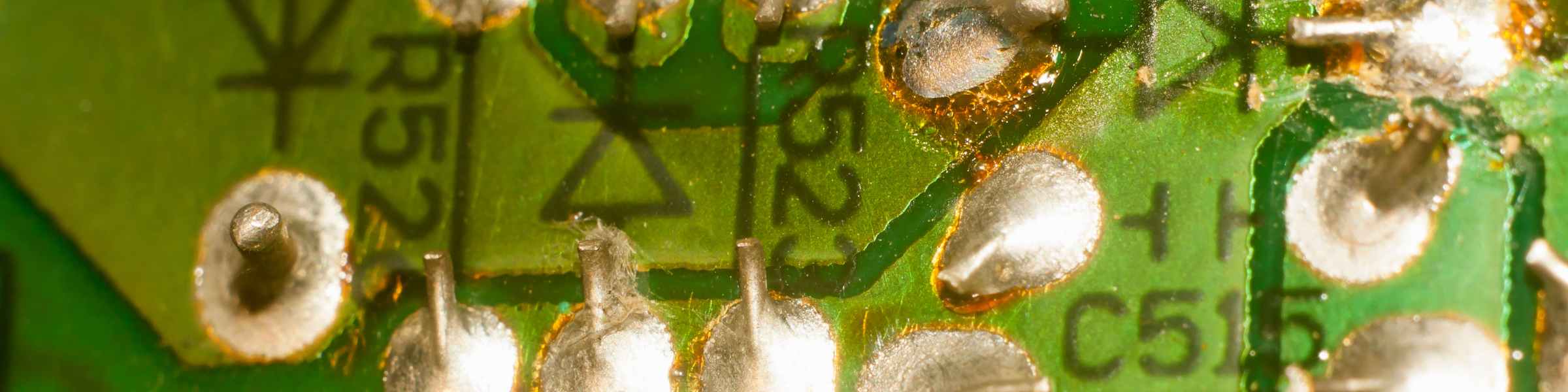
Solder Bridging
Visual Description: Imagine a tiny, unwanted metallic “bridge” of solder forming an electrical connection between two adjacent component pads or pins that should be isolated. This is a solder bridge, and it creates a short circuit that will almost certainly cause the device to malfunction.
Root Causes: The primary cause is an excess of solder paste being deposited or paste flowing where it shouldn’t. This can stem from several sources:
- PCB Design: Pads (land patterns) that are designed too large or too close together for the component’s pitch.
- Stencil Design: The apertures (openings) in the solder paste stencil are too large, allowing too much paste to be deposited.
- Printing Process: Too much pressure on the squeegee during printing can push paste under the stencil, or the stencil itself may be misaligned with the pads.
- Component Placement: A misaligned component can press down on the solder paste, squeezing it out and causing it to bridge with a neighboring pad during reflow.
Prevention: Prevention starts with good design, adhering to IPC standards for land pattern design. It continues with a high-quality, precision-cut stencil and a tightly controlled solder paste printing process, which should be verified by Solder Paste Inspection (SPI).
 1")
Tombstoning
Visual Description: This striking defect affects small, two-terminal passive components like resistors and capacitors. One end of the component lifts off its pad during the reflow process, causing the component to stand vertically, resembling a “tombstone” in a graveyard. This results in an open circuit.
Root Causes: Tombstoning is a classic example of unbalanced forces during solder reflow. The surface tension of the molten solder on one pad overpowers the other, pulling the component up. This imbalance is typically caused by:
- Uneven Heating: One pad reaches reflow temperature significantly before the other, causing the solder to melt and pull first.
- Uneven Pad Design: The pads are not symmetrical in size or shape. A larger pad can act as a heat sink, slowing down the melting process on that side.
- Uneven Solder Paste Deposits: More solder paste on one pad than the other creates a stronger surface tension pull.
Prevention: Symmetrical pad design is crucial. When connecting a pad to a large copper plane, a thermal relief pattern must be used to ensure both pads heat evenly. A precise printing process and a carefully optimized thermal reflow profile are also essential.
 2")
Solder Balls
Visual Description: These are tiny, free-floating spheres of solder that are scattered on the surface of the board, often near passive components, after the reflow process is complete. While they may seem harmless, they can dislodge and cause short circuits later in the product’s life.
Root Causes: Solder balls are typically formed when small amounts of solder paste are squeezed out from under a component and do not properly coalesce with the main solder joint. This can be caused by:
- Moisture: Moisture trapped in the PCB laminate or in the components can outgas violently during reflow, expelling small bits of solder paste.
- Printing Issues: A poor seal between the stencil and the board can cause paste to bleed under the stencil.
- Reflow Profile: A pre-heat stage that is too aggressive (ramping up in temperature too quickly) can cause the flux to spatter, carrying solder particles with it.
Prevention: Proper storage and pre-baking of PCBs and moisture-sensitive components are critical. A well-designed reflow profile and a meticulously controlled printing process are also key preventative measures.
 3")
Insufficient Solder and Open Circuits
Visual Description: This defect appears as a solder joint that has not formed a complete and robust connection, or in the worst case, has no connection at all (an open circuit). The solder fillet will look weak, starved, or non-existent.
Root Causes: An insufficient joint occurs when there isn’t enough solder to form a proper connection. The primary causes include:
- Solder Paste Printing: A clogged aperture in the stencil or insufficient paste being deposited is the most common cause.
- Pad or Component Lead Contamination: Oxidation or other contaminants on the pad or the component’s lead can prevent the solder from properly “wetting” to the surface, causing it to pull back.
- Component Coplanarity: For components with many leads, if the leads are not all perfectly flat (co-planar), some may not make proper contact with the solder paste.
Prevention: A robust SPI process is the best defense against printing issues. Ensuring components and bare boards are fresh and have good solderability is also essential.
 4")
Solder Voids
Visual Description: Solder voids are gas bubbles or pockets trapped within a solder joint after it has solidified. They are often completely invisible from the outside and can typically only be detected with X-ray inspection.
Root Causes: Voids are formed by the outgassing of flux volatiles during the reflow process that get trapped in the solidifying solder. Excessive voiding can compromise the thermal and electrical conductivity of the joint and create stress points that lead to cracking.
Prevention: The primary prevention method is the use of high-quality solder paste with a chemistry designed to minimize voiding, coupled with a carefully optimized thermal reflow profile. The profile must allow enough time and the correct temperature in the “soak” zone for these volatiles to escape before the final reflow spike.
 5")
Head-in-Pillow (HiP)
Visual Description: A particularly challenging defect that affects Ball Grid Array (BGA) components. The solder paste on the pad and the solder ball on the BGA component both melt during reflow but fail to merge into a single, cohesive joint. The result, visible only on X-ray, is a weak connection where the rounded BGA ball appears to be resting in a crater-like depression in the solder on the pad, like a head on a pillow. This creates an unreliable or open connection.
Root Causes: HiP is often caused by dynamic warpage of the component package or the PCB itself during the high temperatures of reflow, causing a momentary separation. Heavy oxidation on the BGA ball can also prevent proper coalescence.
Prevention: A meticulously developed reflow profile designed to minimize thermal gradients and board warpage is the most critical preventative measure. Using high-quality components and solder paste with appropriate flux activity is also vital.
 6")
Prevention Through Partnership: How BENCOR Ensures Quality
Understanding these defects is one thing; consistently preventing them is another. This is where a partnership with a quality-focused CEM makes all the difference. At BENCOR, our entire process is built around proactive defect prevention.
- Proactive Design for Manufacturability (DFM) Feedback: We believe the best way to fix a defect is to design it out from the beginning. Our experienced American engineering team provides thorough DFM feedback on every new design, spotting potential issues like asymmetrical pads that could cause tombstoning or land patterns that are too dense for reliable printing, and suggesting improvements before a single board is ordered.
- Rigorous, Multi-Stage Process Control: We employ a layered quality strategy. It starts with Solder Paste Inspection (SPI) to ensure the foundation of every joint is perfect. Our high-precision, automated pick-and-place machines ensure component accuracy. We develop custom thermal reflow profiles for each unique assembly. And after assembly, we utilize advanced inspection tools like Automated Optical Inspection (AOI) and Automated X-Ray Inspection (AXI) to verify the results with a level of detail that is simply impossible for the human eye.
- The American Standard of Excellence: This meticulous, data-driven, multi-stage approach to defect prevention and detection is a hallmark of high-quality American manufacturing. It’s a philosophy that prioritizes getting it right the first time. It is a deep-seated pride in craftsmanship that extends to the most microscopic details, ensuring the long-term reliability of the final product. This is the standard of quality you can expect when you partner with BENCOR.