

The evolution of wireless communication has been a relentless march toward faster speeds and greater connectivity. 3G brought us mobile data, 4G LTE made video streaming commonplace, and 5G is currently enabling the Internet of Things (IoT) and low-latency applications. Now, on the horizon of 2025 and beyond, the global technology community is actively defining the next frontier: 6G. This next generation promises a quantum leap, with theoretical speeds reaching into the terabits per second (Tbps), near-instantaneous latency, and the power to truly merge our physical and digital worlds through technologies like holographic communication, immersive extended reality (XR), and a globally connected intelligent network. But to achieve this vision, 6G will need to operate in vastly higher frequency bands, moving beyond the gigahertz (GHz) range of today and into the sub-Terahertz (THz) spectrum (e.g., 100 GHz to 300 GHz). At these extreme frequencies, the Printed Circuit Board (PCB) ceases to be a simple platform for components; it becomes a critical, high-performance microwave component in its own right, presenting immense material and design challenges. As a forward-looking American manufacturer, BENCOR understands that supporting the pioneers of 6G requires a deep commitment to quality, precision, and partnership in tackling these formidable engineering hurdles.
The Terahertz Challenge: Why 6G Changes Everything for PCBs
As electrical signals oscillate at hundreds of billions of times per second, their behavior changes dramatically. They begin to act less like simple electrical currents flowing through a wire and more like electromagnetic waves propagating through a medium. This fundamental shift means that standard PCB design rules and materials, which work perfectly well for lower-frequency applications, become completely inadequate.
Extreme Signal Loss (Attenuation)
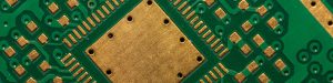
The most significant challenge at THz frequencies is signal loss, or attenuation. Standard PCB laminate materials, like FR-4, are extremely “lossy” at these frequencies. Their molecular structure absorbs and dissipates the energy of the high-frequency signal, effectively killing its strength over even very short distances. A signal that could travel across an entire board at a few megahertz might fade to nothing after just a few millimeters at 200 GHz. This makes conventional materials entirely unsuitable for 6G applications.
The "Skin Effect" and Conductor Surface Roughness
A phenomenon known as the “skin effect” becomes dramatically more pronounced at high frequencies. The electrical current, instead of using the entire cross-section of a copper trace, is forced to travel only on its very outer “skin.” As the frequency increases, this skin depth becomes incredibly thin. Consequently, the microscopic roughness of the copper foil’s surface, which is irrelevant at lower frequencies, becomes a major obstacle course for the signal, scattering the wave and significantly increasing signal loss.
Phase Control and Ultra-Short Wavelengths
At 300 GHz, the wavelength of a signal in a typical PCB dielectric is less than a millimeter. This means that even minuscule variations in the length of a copper trace or slight inconsistencies in the dielectric constant of the board material can cause significant shifts in the signal’s phase. For complex systems like phased-array antennas, which rely on precise timing and phase relationships to steer beams, this lack of control can completely disrupt functionality.
Crosstalk and Electromagnetic Interference (EMI)
The extremely short wavelengths also make it much easier for energy to “leak” or couple from one trace to an adjacent one, leading to severe crosstalk. Furthermore, traces can act as unintentional antennas, radiating energy and creating significant EMI problems that can interfere with other parts of the system or external devices if not meticulously designed and shielded.

Tackling the Challenges: Key Material and Design Strategies for 6G PCBs
Overcoming these THz-level challenges requires a complete rethinking of PCB materials, design, and fabrication.
The foundation of any 6G PCB will be the selection of specialized, ultra-low-loss materials. The two most critical properties are the dielectric constant (Dk) and the dissipation factor (Df, or loss tangent). For 6G, materials must have a very low and extremely stable Dk and a Df that is as close to zero as possible. This has led to intense research and development in materials far beyond FR-4.
Leading candidates include advanced grades of PTFE (Teflon), often reinforced with ceramics or woven glass for mechanical stability; specialized hydrocarbon-ceramic composites; Liquid Crystal Polymers (LCP), which offer excellent properties and flexibility; and even more exotic solutions like glass substrates or bonded-air dielectrics, where air gaps are intentionally created within the PCB structure to serve as the ultimate low-loss insulator.
To combat the skin effect, the use of “low-profile” (LP) or “ultra-low-profile” (ULP) copper foils is non-negotiable. These foils are manufactured to have a much smoother surface finish compared to standard electrodeposited copper. This smoother path for the current significantly reduces conductor losses at THz frequencies, preserving the integrity and strength of the signal.
At these frequencies, traditional microstrip and stripline traces may become too lossy or radiate too much energy. Designers are increasingly turning to more advanced structures that can be integrated directly into the PCB layers. A key example is the **Substrate Integrated Waveguide (SIW)**. An SIW uses two rows of plated vias to create vertical metallic walls within the dielectric material, effectively forming a rectangular waveguide that traps and guides the electromagnetic wave, drastically reducing loss and radiation compared to an open trace.
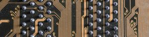
Because the wavelengths are sub-millimeter, the physical tolerances required during PCB fabrication must be incredibly tight. A variation of just a few microns in trace width, spacing, or layer thickness, which might be acceptable in a standard PCB, could completely detune a 6G filter or antenna element. This necessitates the use of the most advanced fabrication technologies, such as Laser Direct Imaging (LDI) for precise pattern transfer and highly controlled etching processes to achieve exact trace geometries.
Connecting an external antenna via a cable is not feasible at THz frequencies, as the cable itself would introduce unacceptable signal loss. Therefore, 6G systems will rely on deep integration of antennas. This includes **Antenna-in-Package (AiP)** designs, where antennas are built directly onto the semiconductor package, and **Antenna-on-Board** designs, where the radiating elements are patterned as part of the PCB’s top copper layer. This requires a seamless co-design process where the RF circuitry and the antenna elements are planned as a single, unified system.
The BENCOR Advantage: Manufacturing Partner for America's 6G Future
While BENCOR may not be formulating the exotic dielectric materials of the future, our role as a high-reliability American electronics manufacturer is crucial in bringing these visionary 6G designs from the lab to reality. The successful assembly of these complex, high-value systems is a critical link in the innovation chain.
Expertise in Handling Advanced and Sensitive Materials
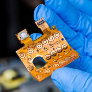
Assembling PCBs made from specialized RF materials like PTFE composites or ceramics requires different processing, handling, and soldering profiles than standard FR-4. These materials can be more sensitive to temperature and mechanical stress. BENCOR’s decades of experience in working with a diverse range of materials ensures that these high-value boards are handled with the care and expertise they demand.
Uncompromising Precision in Assembly
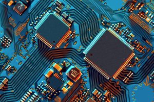
The tiny, sensitive RF components used in 6G systems, along with the tight tolerances of AiP modules, demand the highest level of SMT assembly precision. Solder paste volume, placement accuracy down to the micron level, and perfectly controlled reflow profiles are not just desirable; they are essential for achieving the required RF performance. Our commitment to maintaining state-of-the-art assembly capabilities ensures we can meet these exacting standards.
A Commitment to American Technological Leadership
6G technology is not just a commercial endeavor; it is a matter of national strategic importance. Leadership in 6G will influence everything from economic competitiveness to national security. Ensuring that a robust and capable domestic manufacturing ecosystem exists to support American innovators is vital. BENCOR is proud to be a part of this ecosystem. Partnering with a trusted, capable, and secure US-based CEM ensures that the intellectual property behind this critical technology is protected and that it is built with the unwavering commitment to quality that defines American manufacturing.

Conclusion:
he journey to 6G represents a monumental challenge for the entire electronics industry, particularly for Printed Circuit Board design and manufacturing. It demands a paradigm shift in our approach, pushing us to embrace ultra-low-loss materials, design highly precise circuit structures, and fabricate with unprecedented accuracy. The hurdles of signal loss, skin effect, and phase control at Terahertz frequencies are formidable, but they are being met with incredible innovation. As American engineers and scientists pioneer the technologies that will define our connected future, they will require manufacturing partners who not only understand these challenges but are relentlessly committed to the quality and precision required to overcome them. BENCOR is ready to be that partner, providing the expert assembly services needed to turn the visionary designs of 6G into tangible, reliable reality.